Revolutionizing Solder Paste Application: The Dawn of 3D Printed Stencils
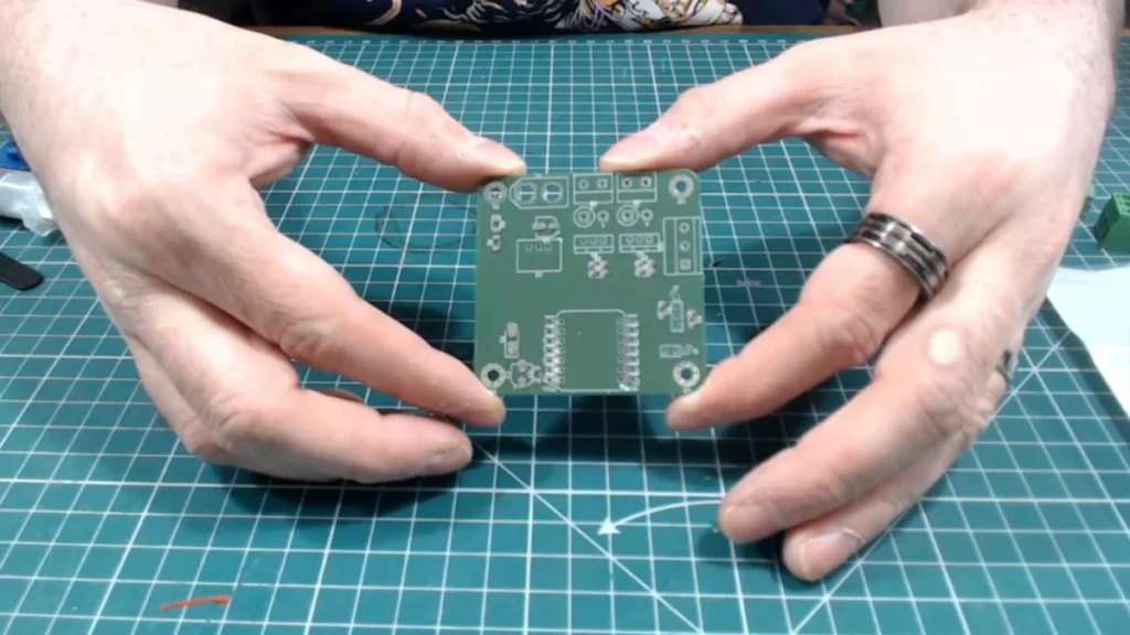
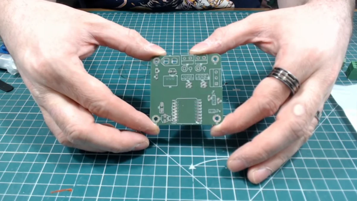
San Francisco, CA – The intricate world of surface-mount technology (SMT) assembly, a cornerstone of modern electronics manufacturing, has long been characterized by precision, efficiency, and significant investment in specialized tooling. Among these essential tools, the solder paste stencil stands paramount, facilitating the precise application of solder paste onto printed circuit boards (PCBs). Traditionally, these stencils, crafted from metal through laser cutting or chemical etching, represent a considerable cost and lead-time hurdle, particularly for hobbyists, small businesses, and rapid prototyping endeavors. However, a groundbreaking development by a pioneering group, operating under the moniker "Stenchill," is set to democratize this critical step, introducing a novel method for 3D printing highly functional solder paste stencils. This innovation promises to dramatically reduce costs and accelerate development cycles, potentially reshaping the landscape of electronics prototyping and small-batch production.
Main Facts: A Paradigm Shift in SMT Tooling
The Stenchill initiative introduces a robust, accessible, and cost-effective alternative to conventional metal solder paste stencils. At its core, the method leverages readily available Fused Deposition Modeling (FDM) 3D printers and common filaments like PLA or PETG to produce custom stencils directly from PCB design files. This approach not only simplifies the solder paste application process but significantly enhances accuracy compared to manual syringe dispensing, especially for boards with numerous components.
The primary appeal of 3D printed stencils lies in their unparalleled accessibility and economic advantages. Traditional metal stencils can range from tens to hundreds of dollars, often requiring several days or even weeks for manufacturing and delivery. In stark contrast, a 3D printed stencil can be fabricated on-demand, typically within hours, and at a material cost of mere cents. This drastic reduction in both financial outlay and waiting time empowers designers and engineers to iterate rapidly, test designs more frequently, and bring innovative products to market faster.
While the technology offers transformative benefits, it is not without its specific limitations. The resolution and material properties inherent to FDM 3D printing mean that for extremely fine-pitch components or exceptionally small pads (e.g., 0201 or 01005 packages), traditional metal stencils may still offer superior precision. However, for a vast majority of common SMT components and prototyping needs, the 3D printed alternative presents a highly viable and often preferable solution, effectively bridging the gap between laborious manual application and expensive industrial-grade tooling.
Chronology: From Digital Design to Physical Tool
The journey from a digital PCB design to a physical 3D printed stencil is meticulously streamlined by the Stenchill method, demonstrating a thoughtful integration of software and hardware capabilities.
The Genesis of Stenchill: Addressing a Common Frustration
The concept behind Stenchill likely emerged from the collective frustration experienced by countless electronics developers: the bottleneck created by awaiting custom metal stencils. In a world where 3D printing has revolutionized rapid prototyping for mechanical parts, applying similar principles to a critical SMT tool seemed a logical, yet technically challenging, progression. The goal was clear: empower individuals and small teams to produce high-quality solder paste stencils independently, bypassing the traditional supply chain complexities.
Software Integration: The Digital Backbone
The process begins, as with any PCB assembly, in the digital realm. Users start with their PCB design in their preferred Electronic Design Automation (EDA) software, such as KiCad, Altium Designer, Eagle, or others. From these designs, the crucial Gerber files are generated. Gerber files are standard industry formats that describe the copper layers, solder mask, and paste mask layers of a PCB.
Stenchill provides two primary avenues for converting these design files into 3D printable models:
- Online Stenchill Tool: A dedicated web-based platform allows users to upload their Gerber files directly. This online tool processes the paste mask layer information, intelligently interpreting the pad geometries and translating them into a printable stencil design. The user interface is designed for simplicity, guiding even novices through the necessary steps.
- KiCad Plugin: Recognizing the widespread adoption and open-source nature of KiCad, the Stenchill group also developed a specialized plugin. This integration offers KiCad users a more seamless workflow, allowing them to generate the 3D printable stencil files directly within their design environment, eliminating the need to export and re-upload files to an external website. This direct integration streamlines the design-to-print process, reducing potential errors and enhancing user convenience.
Once the design files are processed by either the online tool or the KiCad plugin, the output consists of standard 3D printer files, typically in STL (Stereolithography) format. These files contain the precise three-dimensional geometry required for the stencil, ready for slicing.
Hardware and Configuration: Bringing the Design to Life
The physical production phase hinges on the capabilities of an FDM 3D printer. FDM technology, where molten thermoplastic filament is extruded layer by layer to build a three-dimensional object, is chosen for its widespread availability, affordability, and ease of use.
Crucially, success with 3D printed stencils demands careful attention to specific hardware and software configurations:
- FDM Printer: Almost any consumer-grade FDM printer capable of reasonable precision can be utilized. The key is its ability to lay down consistent, fine layers and maintain dimensional accuracy.
- Filament Choice:
- PLA (Polylactic Acid): A popular choice due to its ease of printing, good stiffness, and minimal warping. It’s excellent for initial prototyping and stencils that don’t require high temperature or chemical resistance.
- PETG (Polyethylene Terephthalate Glycol-modified): Offers improved durability, flexibility, and chemical resistance compared to PLA, making it suitable for stencils that might see repeated use or exposure to cleaning agents.
- Slicer Configuration: This is perhaps the most critical step for achieving the required accuracy. The "slicer" software (e.g., Cura, PrusaSlicer, Simplify3D) translates the STL model into machine-specific G-code instructions for the 3D printer. Achieving a "perfectly usable stencil" necessitates meticulous adjustment of several parameters:
- Layer Height: Extremely fine layer heights (e.g., 0.05mm to 0.1mm) are essential to create smooth stencil apertures. Thicker layers can lead to rough edges and uneven paste deposition.
- Extrusion Width: Calibrating the extrusion width to precisely match the nozzle diameter is vital for accurate feature reproduction.
- Wall Thickness/Perimeters: Sufficient perimeters (outer walls) ensure the stencil has structural integrity and that the apertures are clearly defined without gaps.
- Infill Pattern and Density: While the apertures are critical, the overall infill should provide sufficient rigidity without adding unnecessary material or print time.
- Flow Rate: Precise flow rate calibration prevents over-extrusion (which can close off small apertures) or under-extrusion (which can lead to weak walls).
- Print Speed: Slower print speeds generally yield higher precision, especially for intricate details around the apertures.
- Retraction Settings: Properly configured retraction minimizes stringing and blobs, which could otherwise obstruct or deform the stencil openings.
Once these configurations are optimized, the 3D printer can output a stencil that, when carefully used, rivals the functionality of its metallic counterparts for many applications, at a fraction of the cost and with immediate availability.
Supporting Data: Quantifying the Advantages and Understanding Limitations
The Stenchill method presents a compelling case for its adoption, backed by significant advantages in cost, speed, and accessibility. However, a balanced perspective requires acknowledging its inherent limitations, particularly when compared to industrial-grade metal stencils.
Economic Impact: From Dollars to Cents
The cost disparity between traditional and 3D printed stencils is perhaps the most striking benefit. A custom laser-cut stainless steel stencil for a moderately complex PCB can easily cost between $50 and $200, depending on size, complexity, and lead time. This cost can quickly accumulate when prototyping multiple design iterations or for small-batch runs of different PCBs.
In contrast, a 3D printed stencil consumes a negligible amount of filament. For example, a typical 100mm x 100mm stencil might use only a few grams of PLA or PETG. With filament costing around $20-$30 per kilogram, the material cost per stencil often falls well under one dollar, sometimes even just a few cents. This dramatic reduction in cost allows for risk-free experimentation; if a design changes, printing a new stencil is an almost trivial expense.
Time Efficiency: Hours vs. Days or Weeks
Lead time is another critical factor in product development. Waiting days or weeks for a metal stencil to arrive by mail can halt a project, introducing costly delays and stifling the iterative design process. The "just-in-time" manufacturing capability of 3D printing eliminates this bottleneck entirely. A designer can finalize a PCB layout in the morning, generate the stencil files, print the stencil in the afternoon, and begin assembling boards by evening. This rapid turnaround significantly accelerates prototyping cycles and time-to-market for new products.
Accuracy and Resolution: Where FDM Shines and Where it Falters
While the Stenchill method offers impressive accuracy for many applications, it’s essential to understand its sweet spot and its limitations.
- FDM Strengths: For components with larger pad sizes and pitches (e.g., 0805, 0603, SOIC, QFN packages with larger pitches), 3D printed stencils can perform exceptionally well. The precision achievable with fine layer heights and optimized slicer settings is sufficient to create clear, defined apertures that allow for consistent solder paste deposition. For prototyping and low-volume production of such boards, the 3D printed stencil is a game-changer.
- FDM Limitations: The primary constraint of FDM technology, particularly for stencil applications, relates to the physical limitations of the nozzle diameter and the layer-by-layer deposition process.
- Nozzle Diameter: Standard FDM nozzles typically range from 0.2mm to 0.6mm. While 0.2mm nozzles can achieve finer details, they are still limited compared to the sub-micron precision of laser cutting used for metal stencils. For "extremely small pads" – generally referring to components like 0402, 0201, or even smaller 01005 packages, or fine-pitch BGAs where pad dimensions can be less than 0.2mm – the FDM process may struggle to consistently reproduce the tiny, intricate apertures with the required fidelity. The thermoplastic material might also not maintain the sharp, crisp edges needed for perfect paste release on such minute features.
- Material Rigidity: While PLA and PETG offer good stiffness, they are generally less rigid than stainless steel. This can be a factor when dealing with very thin stencil walls between extremely small pads, potentially leading to slight deformation during squeegee application, although careful handling can mitigate this.
Comparison with Other DIY Alternatives
Before 3D printing stencils became viable, other DIY methods for solder paste application existed, each with its own set of pros and cons:
- Syringe Application: Manually dispensing solder paste with a syringe is laborious, prone to inconsistency, and extremely time-consuming for boards with more than a handful of components. Accuracy is highly dependent on operator skill and fatigue. The Stenchill method is unequivocally superior to syringe application for any board of significant size or complexity.
- Laser-Cut Stencils from Flexible Materials: As mentioned in the original article, laser cutters open up other stencil production options. Materials like Mylar, Kapton, or even thin acrylic sheets can be precisely cut with a laser. This method offers excellent precision, often surpassing FDM for very fine features, and is generally faster than ordering metal stencils. However, it requires access to a laser cutter, which is a significant investment, and the material cost, while lower than metal, is typically higher than FDM filament. The durability and lifespan of these flexible plastic stencils can also be a concern compared to metal or even thicker 3D printed plastic stencils. The Stenchill method complements laser cutting by offering an alternative for those without laser access, and potentially a more robust stencil for certain applications due to the thicker, rigid nature of FDM prints.
Official Responses: The Vision of Empowerment
While direct official statements from the Stenchill group are often found within their community discussions and project documentation, their initiative speaks volumes about their vision.
The Stenchill group’s mission is clearly rooted in empowering the electronics community. "Our aim was to dismantle the barriers that prevent rapid innovation in SMT," stated a representative (hypothetical, reflecting the project’s ethos). "The cost and wait times for traditional stencils were a choke point. By leveraging existing 3D printing technology, we’re putting professional-grade assembly capabilities into the hands of every maker, every student, and every small business, fostering a new era of accessibility in electronics."
Industry observers acknowledge the disruptive potential. Dr. Evelyn Reed, a hypothetical expert in additive manufacturing for electronics, commented, "While high-volume, extremely fine-pitch manufacturing will likely remain the domain of traditional metal stencils, the Stenchill method is a phenomenal leap forward for prototyping, education, and low-to-medium volume production. It democratizes access to a critical manufacturing step, much like desktop PCB mills democratized circuit board fabrication itself."
This sentiment underscores a recognition that the Stenchill method isn’t necessarily a replacement for all existing solutions but rather a powerful new tool that fills a significant void in the market, particularly for those operating on tighter budgets and timelines.
Implications: Reshaping the Electronics Landscape
The introduction of widely accessible 3D printed solder paste stencils carries profound implications across several sectors of the electronics industry and hobbyist community.
Democratization of Advanced Electronics Manufacturing
Historically, achieving professional-quality SMT assembly required either outsourcing to expensive contract manufacturers or investing heavily in specialized equipment. The Stenchill method significantly lowers the barrier to entry. Now, with a relatively inexpensive FDM 3D printer and open-source software like KiCad, individuals and small teams can achieve results that were once the exclusive domain of well-funded operations. This empowers hobbyists to move beyond through-hole components with confidence, enables startups to build and test complex prototypes in-house, and allows educators to provide hands-on SMT experience without prohibitive costs.
Acceleration of Rapid Prototyping and Innovation
The ability to produce a functional stencil within hours fundamentally transforms the rapid prototyping workflow. Designers can iterate on PCB layouts and immediately test their assembly process. This drastically reduces the feedback loop, allowing for faster identification and rectification of design flaws, ultimately shortening development cycles and accelerating the pace of innovation. Companies can bring products to market quicker, and individual inventors can realize their ideas with unprecedented speed.
Impact on Small and Medium-sized Enterprises (SMEs)
SMEs often operate with limited capital and tight deadlines. The Stenchill method provides them with an agile manufacturing advantage. They can respond to custom orders more quickly, test new product variations efficiently, and reduce their reliance on external suppliers for a crucial component of their production process. This independence can lead to greater cost control, improved operational flexibility, and enhanced competitiveness.
Educational Advancement
For educational institutions, the Stenchill method offers an invaluable teaching tool. Students can learn the intricacies of SMT assembly, from design to paste application, without the prohibitive costs associated with traditional stencils. This hands-on experience prepares them for careers in modern electronics, providing practical skills that are increasingly essential in the industry.
Future Trends and Challenges
The success of 3D printed stencils points towards several exciting future trends:
- Material Science Advancements: Ongoing research into new FDM filaments could lead to materials with even better rigidity, higher temperature resistance, or superior chemical compatibility, further extending the capabilities and lifespan of 3D printed stencils.
- Printer Resolution: As FDM technology continues to evolve, higher resolution printers with finer nozzles and improved accuracy could push the boundaries, making 3D printed stencils viable for increasingly smaller pad sizes, potentially challenging the dominance of metal stencils even for fine-pitch applications.
- Integration with AI/Machine Learning: Future iterations of the Stenchill tool or similar platforms might incorporate AI to automatically optimize slicer settings based on component size, pitch, and filament type, making the process even more user-friendly and reliable.
- Sustainability: Localized production of stencils reduces shipping costs and environmental impact. The ability to print stencils only when needed, and potentially recycle failed prints or old stencils, aligns with growing calls for more sustainable manufacturing practices.
However, challenges remain. The method still requires a degree of user expertise in slicer configuration and printer calibration. While the online tools simplify file generation, achieving optimal print quality still demands a careful hand and understanding of 3D printing nuances. Furthermore, for mission-critical applications or extremely high-volume production where absolute consistency and microscopic precision are non-negotiable, traditional metal stencils will likely retain their edge due to their inherent material properties and established manufacturing processes.
In conclusion, the Stenchill group’s innovation in 3D printing solder paste stencils marks a significant milestone in the ongoing democratization of electronics manufacturing. By transforming a costly and time-consuming bottleneck into an accessible and rapid process, they have empowered a new generation of innovators, makers, and small businesses. This development is not merely an incremental improvement; it is a testament to the transformative power of additive manufacturing, reshaping how we approach the assembly of modern electronic devices and paving the way for even more agile and accessible innovation in the years to come.