From Junk to Diagnostic Powerhouse: Repurposing 3D Printers for Precision EMI Imaging

In the world of electronics engineering, few challenges are as elusive and frustrating as electromagnetic interference (EMI). Whether it’s a high-speed data line bleeding noise into a sensitive analog sensor or a poorly routed PCB track acting as an unintentional antenna, EMI is the invisible gremlin that keeps engineers awake at night. Traditionally, diagnosing these issues required thousands of dollars in specialized laboratory equipment—anechoic chambers, spectrum analyzers, and near-field probes that were often out of reach for independent makers and small-scale startups.
However, a clever innovation from Clem Mayer, featured on element14 Presents, has democratized this process. By repurposing the precision motion control systems of an obsolete 3D printer, Mayer has engineered a low-cost, automated EMI imager that allows engineers to "see" electromagnetic radiation in real-time. This development represents a significant shift in how we approach PCB debugging and hardware validation.
Main Facts: The Anatomy of the DIY EMI Imager
At its core, Mayer’s project is a masterclass in modular engineering. The system functions by combining three disparate technologies: a CNC-style motion platform, an affordable software-defined radio (SDR) probe, and computer-vision-assisted data visualization.
The Motion Platform
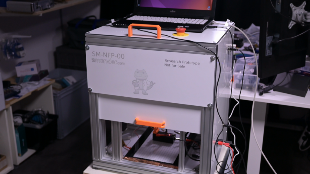
The foundation of the device is a retired 3D printer. While the printer’s original extruding head and heating bed may have reached the end of their operational life, the chassis, stepper motors, and linear rails remain perfectly functional. By stripping away the filament feeder and hot-end, Mayer creates a clean X-Y gantry. This provides the "eyes" of the system with the ability to traverse a two-dimensional grid with sub-millimeter precision, essential for mapping small-scale circuit boards.
The Sensor Suite
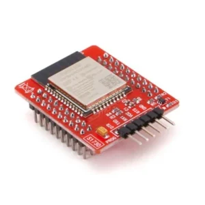
Instead of a plastic extruder, the toolhead is fitted with an EMI probe. This is connected to an RTL-SDR (Software Defined Radio) module. RTL-SDRs, which are widely available and extremely cost-effective, allow the system to "tune in" to specific frequencies of interest. By analyzing the signal strength (dBm) at these frequencies, the system can quantify exactly how much noise is being emitted from specific points on a device under test.
The Control Logic
Orchestrating this movement is an Arduino UNO Rev3 running Grbl 1.1. Grbl is an open-source firmware that translates G-code—the standard language of 3D printers and CNC machines—into physical movement. By sending a serpentine toolpath to the Arduino, the imager systematically scans the entire surface area of the PCB, logging both the XY coordinates and the corresponding EMI strength at each node.
Chronology of Development
The journey to this EMI imager did not happen overnight; it was the result of a deliberate, iterative design process aimed at solving the "visibility gap" in hardware debugging.
- Phase 1: Concept and Sourcing (Early 2026): Mayer identified the primary hurdle in DIY electronics: the lack of visual feedback for signal integrity. Recognizing that 3D printer frames are effectively high-precision coordinate tables, he sourced a defunct unit destined for the landfill.
- Phase 2: Integration of Hardware: The initial build involved modifying the printer’s firmware to accept external G-code commands. The Arduino UNO was chosen for its reliability and its seamless compatibility with Grbl, allowing the team to bypass the printer’s original, proprietary control board.
- Phase 3: The Sensor Interface: The challenge of reading EMI data was solved by utilizing the RTL-SDR as a spectrum analyzer. The team developed a software bridge to record signal levels in sync with the motor movements.
- Phase 4: Overlay Visualization: The final breakthrough came in the software layer. By mounting an overhead camera, the team captured a standard optical image of the PCB. Using a script to correlate the EMI data points with the optical image, they generated a "heat map"—a visual representation where red areas indicate high EMI and blue areas signify quiet zones.
Supporting Data: Why EMI Mapping Matters
To understand the implications of Mayer’s project, one must understand the physics of the problem. EMI isn’t just a "bug"; it is a systemic failure of board-level design.
The Cost of Interference
In the consumer electronics industry, failing EMC (Electromagnetic Compatibility) compliance testing is a disaster. It can lead to expensive product recalls, months of delays, and the necessity of complete PCB redesigns. A single track on a board, if routed incorrectly near a high-frequency clock signal, can turn an entire device into a radiator that violates FCC or CE regulations.
Data Precision
Mayer’s system provides the following data points during a typical scan:
- Spatial Resolution: Limited only by the printer’s stepper motor resolution (often <0.1mm).
- Frequency Range: Determined by the RTL-SDR, typically covering 25MHz to 1.7GHz.
- Signal Intensity: Captured in dBm, allowing for a logarithmic understanding of radiation magnitude.
When this data is converted into a 2D heat map, engineers can pinpoint a "hot spot" to within a few millimeters. This drastically reduces the time required for troubleshooting. Instead of guessing which component is causing a failure, an engineer can look at the heat map and identify the exact inductor or trace length that is behaving like an antenna.
Official Perspectives and Community Response
The response from the Arduino community and the broader engineering world has been overwhelmingly positive. Arduino Team officials have highlighted the project as a prime example of the "circular economy" in engineering—the idea that hardware shouldn’t be discarded simply because its original function is obsolete.
"What Clem Mayer has done is take a ‘dead’ piece of hardware and give it a ‘second life’ as a high-precision scientific instrument," noted a representative from the Arduino community. "This is the essence of open-source engineering. By using an Arduino UNO and some clever software, he has bridged the gap between a hobbyist printer and a professional-grade lab diagnostic tool."
Industry experts have also weighed in, noting that while this device may not replace a full-scale, calibrated anechoic chamber, it is more than sufficient for the "pre-compliance" phase of design. By catching issues early in the prototyping stage, engineers can save thousands of dollars in lab rental fees and consulting costs.
Implications: The Future of DIY Diagnostics
The success of the "3D Printer to EMI Imager" conversion has profound implications for the future of small-scale hardware development.
Democratization of Engineering Tools
As professional equipment becomes increasingly expensive, the DIY approach to instrumentation is becoming a necessity rather than a novelty. Projects like this suggest a future where "diagnostic stations" are built from repurposed machines, allowing independent developers to compete with large corporations in terms of testing capabilities.
Environmental Impact
By extending the lifecycle of 3D printers, this project also addresses the growing problem of e-waste. Instead of upgrading to the latest, most expensive 3D printer and discarding the old one, engineers are incentivized to maintain and repurpose their hardware. This ethos of repairability and repurposing is gaining traction globally, supported by platforms like element14.
Educational Value
For students and hobbyists, this imager is an invaluable teaching tool. It transforms an abstract, invisible phenomenon—electromagnetism—into something concrete and visual. It teaches users not just how to solder or code, but how to think about signal integrity, PCB layout, and the physical constraints of electronic systems.
Future Iterations
The project is already sparking a conversation about future improvements. Potential upgrades mentioned by the community include:
- 3D Scanning: Moving the sensor in the Z-axis to create 3D EMI intensity maps.
- Automated Shielding Tests: Using the system to test the effectiveness of different metal enclosures and shielding materials.
- AI-Assisted Debugging: Integrating machine learning to automatically flag specific components (like buck converters or microcontrollers) that frequently cause EMI issues.
Conclusion
The transformation of a dusty, unused 3D printer into a state-of-the-art EMI imager is more than just a clever hack; it is a blueprint for the future of hardware engineering. By combining legacy hardware with modern, affordable software-defined radio and open-source control boards, Clem Mayer has demonstrated that the most powerful tools in engineering are often those we build ourselves.
For the engineer facing the nightmare of intermittent noise, the solution may not lie in a million-dollar lab, but in the corner of their own workshop. As we look toward an era of increasingly complex and compact electronics, the ability to visualize the invisible will become a fundamental skill. Thanks to this project, that capability is now within the reach of anyone with an old printer and a bit of ingenuity.