Unveiling the True Carbon Footprint of Silicon: How Raspberry Pi Recalibrated Its Life Cycle Assessments
In the evolving landscape of sustainable technology, calculating the environmental impact of hardware has traditionally relied on generalized metrics. For years, companies striving for transparency have measured emissions through mass, weighing physical components and mapping those figures against broad databases. However, as organizations dig deeper into their supply chains, the limitations of these macro approaches are becoming glaringly apparent.
In a recent and significant methodological breakthrough, Raspberry Pi—the globally renowned creator of affordable, high-performance computing hardware—discovered that its traditional carbon accounting methods significantly overestimated the embodied carbon of its products. By moving away from weight-based approximations and embracing advanced academic modeling, the company achieved a startling revelation: its actual hardware footprint is roughly 30% lower than previously reported.
This deep dive explores how Raspberry Pi transitioned from generic industry estimates to precise silicon-level carbon accounting, the academic partnerships that made it possible, and what this paradigm shift means for the future of sustainable electronics manufacturing.
Main Facts: The 30% Revelation
The core finding of Raspberry Pi’s recent methodological overhaul is both counterintuitive and encouraging: the company was carrying a heavy "ghost footprint" in its official reporting simply because its carbon tracking tools were not built for the minute intricacies of semiconductor manufacturing.
When conducting a Life Cycle Assessment (LCA), manufacturers typically weigh every component—from the printed circuit board (PCB) to the housing and connectors—and map those metrics to established environmental databases like ecoinvent. While this weight-based methodology works exceptionally well for standardized materials like aluminum, steel, and plastics, it fails entirely when applied to advanced silicon microchips.
A microprocessor’s carbon footprint is not dictated by how heavy it is; rather, it is a function of highly complex variables:
- The Process Node: The microscopic scale of the transistors (e.g., 28nm, 16nm, 7nm).
- Die Area: The physical surface area of the silicon chip.
- Manufacturing Complexity: The number of masking and etching steps required.
- Fab Energy Intensity: The specific energy consumption of the semiconductor fabrication plant (fab).
- Manufacturing Yield: The percentage of working chips produced versus defective ones discarded during the process.
By treating its custom silicon as generic mass, Raspberry Pi had previously relied on conservative, broad-brush semiconductor datasets. While this guaranteed that their previous LCAs were safely erring on the side of caution, "conservative" is not synonymous with "accurate."
When the company finally applied precision modeling to its silicon components—specifically utilizing the advanced MicroGreen and ACT (Architectural Carbon Modeling Tool) frameworks developed by researchers at Cornell University, Columbia University, Harvard, and Meta—the results were transformative. Without altering the physical manufacturing process, supply chain, or product designs in any way, Raspberry Pi’s overall product LCAs dropped by approximately 30%. The phantom emissions simply vanished, replaced by hard, mathematically grounded reality.
Chronology: From Inventory Weight to Silicon Precision
To understand how Raspberry Pi arrived at this watershed moment, it is necessary to trace the chronology of the company’s sustainability journey and its intersection with cutting-edge academic research.
Phase 1: The Traditional LCA Approach
In earlier stages of its environmental accountability reporting, Raspberry Pi established a transparent framework for calculating the embodied carbon of its single-board computers and microcontrollers. This involved systematically weighing each individual component on the bill of materials, cross-referencing those weights with the ecoinvent database, and collaborating directly with manufacturing partners to assemble a comprehensive life cycle assessment.
While this approach provided a solid, tangible foundation, the engineering and sustainability teams found themselves increasingly unsettled by one specific anomaly in the data: silicon.
Phase 2: Identifying the Silicon Blind Spot
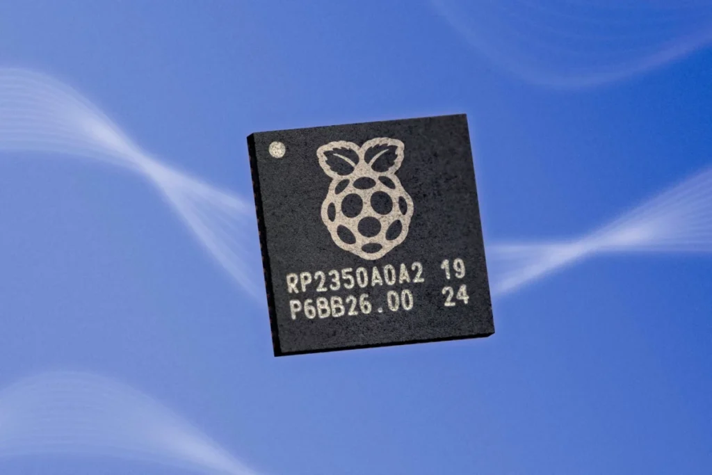
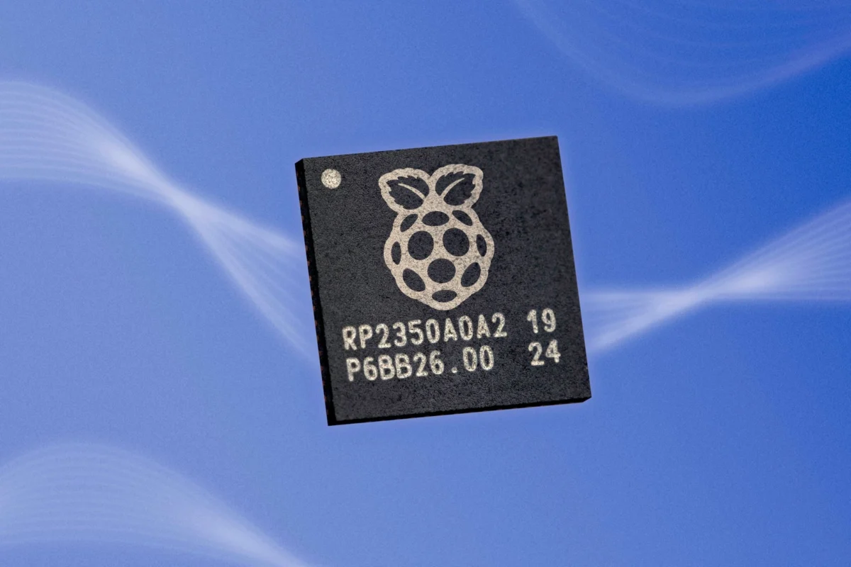
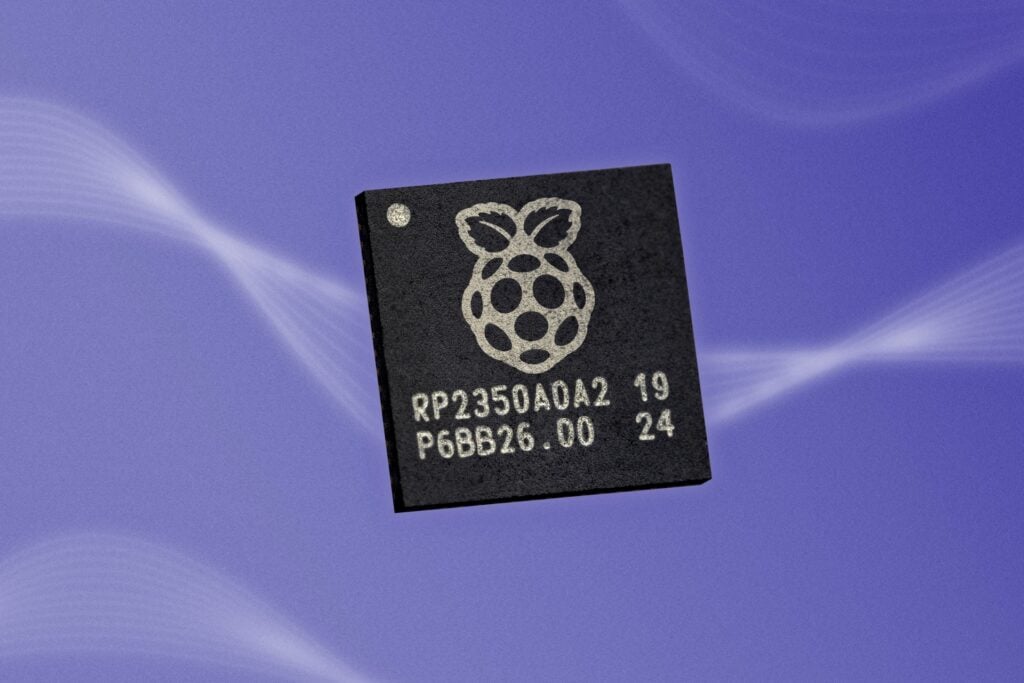
As the team looked closer at their LCA results, the weight-based metrics for semiconductor components began to look fundamentally flawed. Silicon chips weigh mere fractions of a gram, yet under legacy mass-mapping systems, they were carrying disproportionate environmental burdens. The team recognized that a generic semiconductor dataset could not accurately capture the nuance of a custom-designed microcontroller like the RP2350 or its predecessors. They knew their numbers were conservative, but the lack of granularity began to undermine the precision of their internal design and sourcing decisions.
Phase 3: The Academic Breakthrough (MicroGreen and ACT)
Salvation came from the halls of academia. Researchers at Cornell University and Columbia University had developed MicroGreen, a groundbreaking software tool designed to model the embodied carbon of hardware components. MicroGreen itself builds upon the Architectural Carbon Modeling Tool (ACT), an earlier framework developed collaboratively by researchers at Harvard University and Meta.
Engineered specifically to treat carbon emissions as a first-order design constraint—right alongside computational performance, thermal limits, and power consumption—MicroGreen allows engineers to bypass crude weight approximations. Instead, it calculates a chip’s carbon footprint based on its actual physical and operational properties: die size, node technology, fab energy mix, and yield rates.
Phase 4: Collaborative Implementation
Recognizing the potential of the tool, Raspberry Pi initiated a direct collaboration with the academic minds behind the software—specifically Udit Gupta, Ariel Goldner, and Xuesi Chen.
Instead of relying on theoretical assumptions, the research team worked hand-in-hand with Raspberry Pi engineers to input the exact specifications of the custom silicon chips deployed in actual production lines. By matching the MicroGreen model directly to the hardware being shipped to millions of makers, educators, and industrial users worldwide, the collaborators successfully bridged the gap between theoretical laboratory research and industrial-scale manufacturing.
Supporting Data and the Mechanics of Semiconductor Carbon
To fully grasp why weight-based LCA fails for semiconductors, one must understand the staggering resource intensity of microchip fabrication.
The Anatomy of Semiconductor Footprints
Semiconductor fabrication facilities (fabs) are among the most energy- and resource-intensive industrial environments on Earth. Creating a silicon wafer involves:
- Ingot Growth and Slicing: Purifying electronic-grade silicon into large monocrystalline ingots and slicing them into ultra-thin wafers.
- Photolithography: Repeatedly exposing the silicon to ultraviolet light through complex photomasks to etch microscopic circuits. This process requires ultra-clean environments (cleanrooms) that run massive HVAC and air-filtration systems 24 hours a day.
- Chemical Vapor Deposition and Etching: Utilizing specialized greenhouse gases (such as perfluorocarbons or PFCs) for etching and chamber cleaning, which have extraordinarily high global warming potentials (GWPs).
Because of these complex processes, two silicon chips of the exact same physical weight can have vastly different carbon footprints. A chip produced on an older, less efficient 40nm process node in a coal-heavy energy grid will have a significantly higher embodied carbon profile than a smaller, more advanced die produced on a modern 5nm node powered by renewable energy—even if they tip the scale at the exact same weight.
The Impact on Product-Level LCAs
When Raspberry Pi integrated MicroGreen into its assessment pipeline, the removal of inflated silicon estimates resulted in a systemic 30% reduction across the board for product-level LCAs.
This drop does not mean that the hardware suddenly became greener overnight; rather, it highlights a historical accounting error inherent to the electronics industry at large. For years, consumer electronics companies may have been artificially inflating their scope 3 emissions (specifically embodied carbon) simply because the tools available could not accurately parse the microscopic reality of silicon.
Official Responses and Perspectives
The partnership between Raspberry Pi and the academic creators of MicroGreen represents a powerful intersection of open-source ethos, academic rigor, and industrial pragmatism.
The Academic Perspective
Reflecting on the collaboration, the research team from Cornell Tech and Columbia University emphasized the value of testing laboratory innovations in real-world environments:
"Collaborating with Raspberry Pi has shown us how a tool developed in the lab can be applied to sustainability questions at production scale. Applying MicroGreen to the Raspberry Pi actually grounds our research in reality and dramatically increases the impact our work can have."
For academic researchers, access to Raspberry Pi’s transparent supply chain data and high-volume production metrics provided a unique testing ground to validate whether theoretical carbon models hold up under commercial pressure. The success of the implementation proves that academic carbon modeling tools are ready for prime-time industrial deployment.
The Raspberry Pi Perspective
From Raspberry Pi’s standpoint, the partnership resolved a lingering professional and ethical dilemma. For a company that prides itself on democratizing computing while remaining conscious of resource utilization, having inaccurate environmental data was unacceptable.
In their official commentary, leadership noted:
"A more accurate model isn’t just about a lower headline number; it ensures the figures we report reflect reality, and that the decisions we make from here in design, sourcing, and where we focus our efforts are built on firm ground."
The company extended formal gratitude to Udit Gupta, Ariel Goldner, and Xuesi Chen, acknowledging that their collaborative work has fundamentally elevated the integrity of Raspberry Pi’s carbon reporting framework.
Implications for the Tech Industry
The implications of this breakthrough extend far beyond Raspberry Pi’s product lineup. As the global technology sector faces increasingly stringent environmental regulations, carbon taxes, and consumer demands for true transparency, the methodology of carbon accounting must evolve.
1. The Death of "Mass-Based" Electronics LCA
For decades, sustainability auditors have relied on macro-level input-output models and weight-based heuristics for electronic assemblies. Raspberry Pi’s experience demonstrates that these legacy methods can introduce massive margins of error—often in the direction of overestimation. If a low-cost, high-volume hardware manufacturer can shave 30% off its embodied carbon profile simply by adopting proper silicon modeling, thousands of other electronics manufacturers may similarly find that their reported footprints are distorted.
2. Carbon as a First-Class Engineering Metric
By utilizing tools like MicroGreen and ACT, hardware designers can begin treating carbon emissions the same way they treat silicon area, clock speed, and power draw. When carbon is integrated into the computer-aided design (CAD) and chip architecture phases, engineers can make informed trade-offs. For example, they can evaluate whether moving to a smaller process node—which requires more intensive fab energy upfront but yields higher energy efficiency during the product’s operational lifetime—makes environmental sense across the entire lifecycle.
3. A Blueprint for Academic-Industrial Synergy
Finally, this collaboration serves as a shining example of how applied research can immediately benefit commercial sustainability efforts. Too often, academic software tools remain locked inside university repositories, failing to cross the chasm into commercial adoption. By opening channels between Cornell/Columbia researchers and a hardware manufacturer like Raspberry Pi, both parties achieved their goals: the researchers validated their model at scale, and the manufacturer gained scientific clarity over its supply chain.
Conclusion
Raspberry Pi’s recalibration of its silicon carbon footprint is a milestone moment for sustainable hardware engineering. By discarding crude weight-based approximations and embracing the granular physics of semiconductor manufacturing through the MicroGreen and ACT tools, the company has corrected a vital blind spot in its environmental accounting.
As other technology firms take note, this breakthrough signals the end of the era of generic, back-of-the-envelope carbon estimations for microchips. Moving forward, precision, academic collaboration, and silicon-level modeling will be the bedrock upon which truly sustainable electronics are built.