Beyond the Scale: How Raspberry Pi Redefined Silicon Carbon Accounting
By Tech & Sustainability Desk
Published: August 2026
Main Facts
In a significant update to its environmental accounting practices, Raspberry Pi has announced a dramatic downward revision in the calculated embodied carbon footprint of its hardware products. By shifting away from traditional weight-based emission estimates and adopting an advanced, process-aware semiconductor modeling framework, the company has successfully reduced its overall product Life Cycle Assessments (LCAs) by approximately 30%.
The breakthrough stems from a direct collaboration with academic and industry researchers who developed MicroGreen and the Architectural Carbon Modeling Tool (ACT). Originally engineered at institutions including Cornell University, Columbia University, Harvard University, and Meta, these tools allow hardware designers to calculate silicon emissions based on physical and operational parameters—such as die area, manufacturing yield, process nodes, and semiconductor foundry energy intensity—rather than relying on generalized weight mappings.
According to Raspberry Pi, the transition addresses a long-standing flaw in electronics sustainability reporting: treating microchips like generic commodities. While the company’s previous methodology yielded a safe, conservative estimate, it fundamentally distorted reality, artificially inflating the true environmental cost of the silicon powering millions of single-board computers worldwide.
Chronology: From Weight-Based Guesswork to Precision Modeling
To understand the significance of this shift, one must examine the evolution of Raspberry Pi’s sustainability reporting and the timeline of how semiconductor carbon accounting has matured over the past decade.
Phase 1: The Traditional Life Cycle Assessment (LCA) Approach
In earlier sustainability disclosures, Raspberry Pi established its baseline carbon footprint through a standard, globally recognized methodology. This process involved:
- Meticulously weighing every individual component soldered onto a board.
- Mapping those material weights to the established ecoinvent database, a premier repository for life cycle inventory data.
- Partnering with supply chain stakeholders to aggregate transport, assembly, and end-of-life parameters.
For passive components, plastics, and printed circuit board (PCB) substrates, this weight-to-emissions mapping proved exceptionally reliable. However, as the engineering team scrutinized the resulting data, a persistent anomaly kept recurring around the most technologically complex component on the board: silicon.
Phase 2: The Silicon Blind Spot
Standard LCA frameworks operate largely on mass balance. If an item weighs x grams, it is assigned a corresponding carbon value based on industry-average material extraction and processing emissions.
For semiconductors, however, mass is an entirely misleading metric. A high-performance, energy-intensive silicon die requires an immense amount of ultra-pure resources, cleanroom operations, multi-layered photolithography steps, and specialized chemical processing, all condensed into a fraction of a gram. Conversely, a heavier, older-node chip might consume fewer advanced manufacturing cycles.
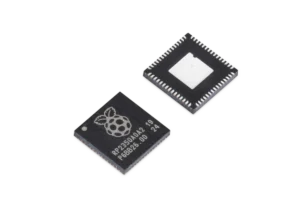
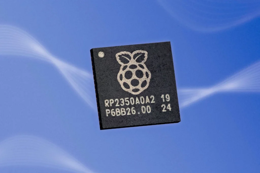
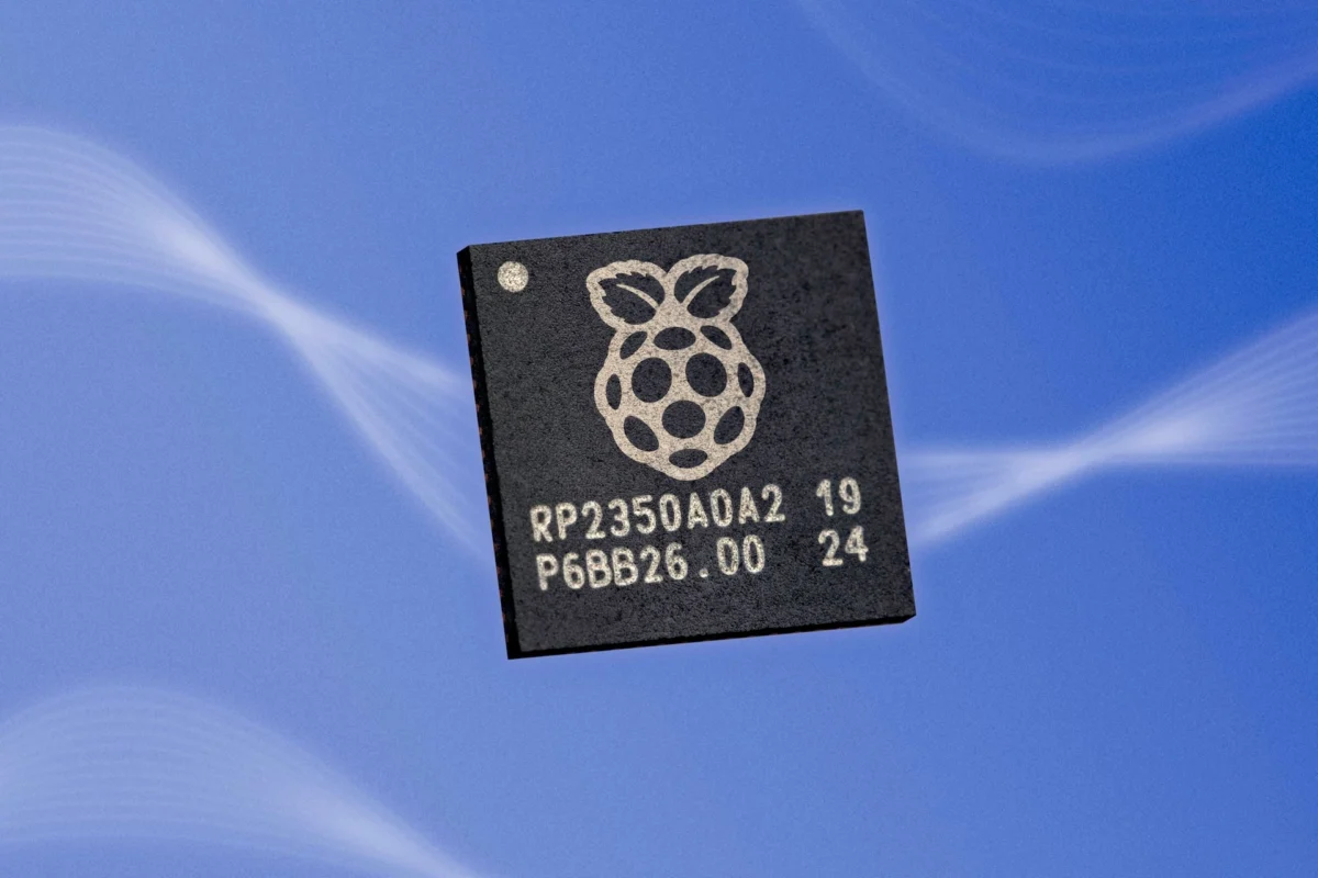
Treating Raspberry Pi’s custom silicon—such as the RP2350 microcontroller—as generic mass forced the company to rely on broad semiconductor datasets. The resulting carbon figures were undeniably conservative, but they lacked scientific precision.
Phase 3: The Academic Breakthrough (MicroGreen and ACT)
The solution arrived from cutting-edge academic research. Researchers at Harvard and Meta originally developed ACT (Architectural Carbon Modeling Tool), which was subsequently expanded into MicroGreen by teams at Cornell Tech and Columbia University.
Designed specifically to integrate sustainability into the earliest phases of hardware engineering, MicroGreen elevated carbon to a "first-order design consideration," sitting right alongside clock speed, power consumption, and thermal dissipation.
Phase 4: Production-Scale Integration
Recognizing the potential of the tool, Raspberry Pi initiated a direct partnership with researchers Udit Gupta, Ariel Goldner, and Xuesi Chen. Together, the teams bridged the gap between theoretical laboratory models and high-volume, commercial production lines. By feeding exact specifications of Raspberry Pi’s proprietary silicon into MicroGreen, the companies replaced industry averages with real-world fabrication data, culminating in the 30% reduction in total product LCA figures announced this year.
Supporting Data: Dissecting the Semiconductor Carbon Equation
To appreciate why a weight-based approach fails in modern electronics, it is vital to examine the specific variables that dictate a microchip’s true environmental footprint.
The Flaw of Mass-Based Metrics
In standard environmental reporting, emissions are frequently expressed per kilogram of material ($kg text CO_2texte/kg$). For bulk materials like aluminum or copper, this correlation is linear and predictable.
For semiconductors, the relationship between weight and emissions is virtually non-existent. Consider the following microchip characteristics that dictate carbon intensity:
- Process Node Technology: Transitioning from older manufacturing nodes (e.g., 40nm) to advanced nodes (e.g., 7nm or smaller) exponentially increases the number of lithography masks, chemical vapor deposition cycles, and plasma etching steps. Each additional layer compounds the energy consumed inside the cleanroom fab.
- Die Area: The physical surface area of the silicon slice dictates how many functional chips can be cut from a single 300mm wafer. Smaller dies yield more chips per wafer, drastically amortizing the massive upfront energy cost of growing and slicing the initial silicon ingot.
- Manufacturing Yield: Not every die manufactured on a wafer functions perfectly. Yield rates (the percentage of working chips) mean that defective silicon must be factored into the embodied carbon of the surviving, shipped units. A low-yield run dramatically spikes the carbon footprint of every successful chip.
- Fab Energy Intensity: Not all semiconductor fabrication plants (fabs) are created equal. The energy mix of the local electrical grid powering the cleanroom—whether heavily reliant on coal, natural gas, or renewable geothermal/hydroelectric energy—plays a massive role in the final emissions profile.
The Impact on Product LCAs
When Raspberry Pi applied MicroGreen to its hardware lineup, the removal of generalized semiconductor inflation revealed that previous estimates had significantly overcalculated the silicon’s share of the total footprint.
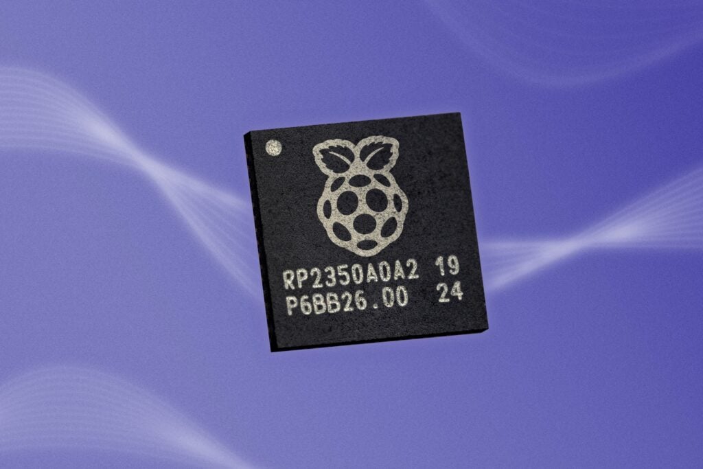
Because the physical weight of a silicon die is negligible, the old models relied on worst-case scenario assumptions from generalized electronics databases. Once the tool accounted for actual die sizes, efficient yields, and precise node architectures, the overall product LCA dropped by approximately 30%.
Crucially, Raspberry Pi emphasizes that this reduction did not occur because the physical products were redesigned, re-engineered, or manufactured with cleaner materials overnight. Rather, the drop represents a correction in epistemic accuracy: the emissions were never actually there in the first place; they were artifacts of an imprecise measurement tool.
Official Responses and Collaborative Insights
The success of this initiative highlights a rare and highly effective synergy between academic research institutions and commercial hardware manufacturers.
Perspectives from Cornell Tech and Columbia University
Reflecting on the collaboration, the research team behind MicroGreen—led by Udit Gupta, Ariel Goldner, and Xuesi Chen—released a joint statement underscoring the importance of real-world validation:
"Collaborating with Raspberry Pi has shown us how a tool developed in the lab can be applied to sustainability questions at production scale. Applying MicroGreen to the Raspberry Pi actually grounds our research in reality and dramatically increases the impact our work can have."
For academic engineers, testing theoretical models against the chaotic, high-volume realities of global supply chains is often the ultimate bottleneck. By opening its production data to the creators of MicroGreen, Raspberry Pi provided an invaluable testing ground that helps validate the tool for the broader semiconductor industry.
Raspberry Pi’s Leadership Perspective
Raspberry Pi leadership echoed this enthusiasm, emphasizing that transparency and precision must take precedence over comfortable, conservative accounting.
In official commentary, the company noted:
"A more accurate model isn’t just about a lower headline number; it ensures the figures we report reflect reality, and that the decisions we make from here in design, sourcing, and where we focus our efforts are built on firm ground."
The company formally extended its gratitude to Gupta, Goldner, and Chen, noting that their dedication to open, rigorous carbon modeling has permanently elevated the standard of the hardware industry’s environmental reporting.
Implications for the Tech Industry
The implications of Raspberry Pi’s transition extend far beyond a single hardware manufacturer. As global climate regulations tighten and consumers demand genuine, verifiable transparency regarding product lifecycles, the electronics industry faces mounting pressure to clean up its reporting standards.
1. Moving Beyond "Greenwashing" Through Over-Estimation
Historically, companies have often preferred to lean on conservative, high-side estimates to avoid accusations of underreporting emissions. However, as Raspberry Pi demonstrates, carrying inflated figures distorts internal corporate decision-making. If a company believes its silicon is responsible for an unrealistic share of its carbon footprint, engineering and procurement teams might misallocate capital toward solving non-existent problems, while ignoring actual high-impact areas.
2. Setting a New Open Standard for Semiconductor Design
By embracing tools like MicroGreen and ACT, Raspberry Pi is helping pave the way for carbon modeling to become a standard computer-aided design (CAD) metric. Just as engineers simulate electrical resistance and thermal dissipation before taping out a chip, future semiconductor designers will be able to simulate carbon emissions at the architectural level.
3. Supply Chain Accountability
As more companies adopt process-aware modeling, pressure will shift directly onto semiconductor foundries (such as TSMC, GlobalFoundries, and UMC) to provide transparent, granular data regarding fab energy usage, chemical inputs, and yield metrics. This creates a positive feedback loop: as foundries compete on sustainability, the foundational data feeding tools like MicroGreen will become even more precise, driving real-world decarbonization across the entire electronics supply chain.
Conclusion
Raspberry Pi’s collaboration with the creators of MicroGreen marks a watershed moment in hardware sustainability. By trading blunt, weight-based heuristics for surgical, process-aware modeling, the company has not only slashed its reported LCA figures by 30% but has also established a gold standard for carbon accounting accuracy.
In an industry prone to greenwashing and generalized estimates, Raspberry Pi’s willingness to scrutinize its own data—and partner with academia to correct it—proves that true sustainability begins with the courage to measure reality as it is, rather than how it appears on a scale.