Beyond Silicon: The In-Situ Revolution in Atomic-Scale Transistor Fabrication
The semiconductor industry has spent over half a century chasing the ghost of Gordon Moore, shrinking transistors to ever-smaller dimensions to fuel the digital age. However, as we approach the physical limits of traditional silicon fabrication, the industry faces a daunting "scaling wall." A breakthrough research effort led by Seok Young Min and his team, recently published in Science, suggests a radical departure from conventional manufacturing: building transistors in-situ directly from a single, atomic-layer material. This paradigm shift could move us away from the additive, multi-step lithography processes of today toward a future of monolithic, atomic-scale circuitry.
Main Facts: The End of Grafting
Traditionally, manufacturing a MOSFET (Metal-Oxide-Semiconductor Field-Effect Transistor) is a complex, additive process. It involves layering silicon, depositing gate oxides, doping regions with different impurities, and grafting metal contacts—all of which require precise, multi-step alignment. Each added layer introduces structural defects, thermal expansion mismatches, and alignment errors that limit the ultimate density of the chip.
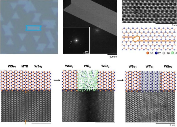
The research conducted by Min et al. bypasses this "grafting" complexity entirely. By utilizing a monolayer of tungsten ditelluride (WTe₂), the team demonstrated that they could selectively convert parts of the material into functional components. Through controlled chemical modification, the researchers transformed specific segments of the WTe₂ monolayer into:
- Insulators: Tungsten oxide (WOₓ) was formed to act as the dielectric barrier.
- N-type Semiconductors: Specific regions were converted into tungsten disulfide (WS₂).
- P-type Semiconductors: Other sections were engineered into tungsten diselenide (WSe₂).
By creating these distinct electronic regions—p-type, n-type, and insulating—within a single, continuous sheet of material, the researchers successfully fabricated a functional MOSFET without ever needing to introduce external "foreign" materials to form the transistor junction. This monolithic approach preserves the structural integrity of the 2D lattice, potentially allowing for device densities that dwarf current industry standards.
Chronology: A Decade of 2D Exploration
The path to this breakthrough was not overnight; it is the culmination of over a decade of intensive research into two-dimensional (2D) materials.
- 2010–2014: The Rise of TMDCs: After the discovery of graphene’s unique properties, the scientific community shifted focus toward Transition-Metal Dichalcogenides (TMDCs). Unlike graphene, which lacks a natural bandgap, TMDCs possess an intrinsic semiconductor bandgap, making them ideal candidates for transistor channels.
- 2014: Early Foundations: N. Lu and his colleagues published foundational research exploring how MoSe₂ (molybdenum diselenide) could be manipulated for semiconductor applications. This work proved that 2D materials could be engineered at the atomic level, providing the theoretical bedrock for the "in-situ" concept.
- 2015–2022: Refinement of Control: Researchers spent years refining methods for "phase engineering"—the process of switching the electronic properties of a material without changing its overall chemical composition. Techniques such as laser-assisted oxidation and chemical vapor transport became standard in laboratories worldwide.
- 2026: The Breakthrough: The report by Min et al. represents the first successful demonstration of a fully integrated transistor device created through the localized, selective transformation of a single TMDC monolayer. This achievement transitions the field from "can we change the material" to "can we build a functional computer with it."
Supporting Data: Why WTe₂ Matters
The choice of WTe₂ as the base material is strategic. WTe₂ is a semimetal that exhibits complex quantum properties and can be thinned down to a single atomic layer—a "monolayer"—without losing its structural stability.
In industrial semiconductor fabrication, the "pitch" (the distance between transistors) is limited by the alignment of multiple masks and the physical deposition of materials. In the method proposed by Min et al., the transistor is "grown" or "converted" in place. Because the conversion is chemical and localized, the resolution is limited only by the precision of the stimulus (such as a focused laser or electron beam).
Data from the study indicates that these in-situ devices exhibit excellent switching behavior (on/off ratios), which is the primary metric for digital logic. Furthermore, because there are no interfaces between different materials—everything is part of the same original lattice—the scattering of electrons at junctions is minimized. This suggests that these atomic-scale transistors could not only be smaller but also significantly faster and more energy-efficient than their silicon counterparts.
Official Responses and Peer Perspectives
While the semiconductor industry has remained cautious about moving away from silicon, the academic response to the Science publication has been overwhelmingly positive.
"This is the Holy Grail of 2D electronics," noted one lead researcher in the field of condensed matter physics. "The ability to perform ‘subtractive’ or ‘transformative’ manufacturing on a monolayer is a radical departure from the ‘additive’ logic of the last fifty years. However, the challenge remains: scale."
The primary concern raised by industry analysts is the transition from a laboratory bench to a multi-billion dollar fabrication facility (fab). Silicon manufacturing is deeply entrenched in "Extreme Ultraviolet" (EUV) lithography. Changing the entire production line to accommodate TMDC conversion requires a complete reimagining of the lithographic process.
Proponents argue, however, that the cost savings from eliminating the complex, multi-layer deposition steps could eventually offset the capital expenditure of building new facilities. By reducing the number of processing steps from hundreds to a fraction of that, the yield (the number of functional chips per wafer) could increase dramatically, potentially lowering the cost-per-transistor.
Implications: The Future of Computing
The implications of this research are far-reaching, touching upon several key areas of technological development:
1. The Death of the "Scaling Wall"
As silicon transistors approach the 2nm and 1nm thresholds, quantum tunneling makes it increasingly difficult to keep electrons where they belong. TMDCs, with their atomic thickness, provide a superior alternative for gate control, effectively pushing the physical limit of scaling by another several decades.
2. Monolithic 3D Integration
Current chips are essentially 2D, even if they are stacked. With in-situ engineering, it may become possible to create 3D circuitry where layers are grown directly on top of each other through controlled chemical transformations. This would allow for a massive increase in computational density, potentially enabling true neuromorphic (brain-like) computing architectures.
3. Sustainability in Manufacturing
The current semiconductor industry is incredibly resource-intensive, requiring vast amounts of high-purity chemicals and energy for deposition and cleaning. If manufacturing can be reduced to the transformation of a single monolayer of material, the environmental footprint of the chip industry could be significantly reduced, moving toward a "green" fabrication model.
4. Beyond Computing
While the focus is on MOSFETs, the ability to transform TMDCs at the atomic level has applications in sensors, flexible displays, and quantum computing. A single sheet of TMDC could theoretically host a sensor array, a logic processor, and a communication interface, all fabricated through the same in-situ process.
Conclusion
The research provided by Seok Young Min et al. is a stark reminder that silicon is not the end of the road for computing. While the transition from research to commercial reality is a long and arduous process, the proof-of-concept for in-situ transistor fabrication provides a clear map for the next generation of electronics. By looking toward atomic-layer engineering, the industry may finally find a way to break free from the constraints of the 20th century and enter a new era of nano-electronics. The future of the chip, it seems, may not be in what we add to the wafer, but in how we transform the wafer itself.