From Silicon Dreams to Silicon Reality: The Democratization of Chip Fabrication
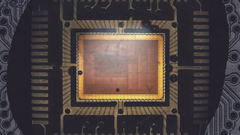
For decades, the realm of integrated circuit (IC) fabrication was an exclusive club—a domain reserved for multi-billion-dollar corporations, state-sponsored research labs, and the giants of the semiconductor industry. To "tape out" a custom chip was a feat of logistics and finance that effectively precluded the hobbyist, the independent engineer, and the small startup. However, a quiet revolution is unfolding. Following the emergence of accessible shuttle services like Tiny Tapeout, a new player, wafer.space, has pushed the envelope further, enabling individual designers to move from RTL code to physical silicon.
A recent technical deep-dive by the creator known as [Breaking Taps] has showcased the tangible reality of this shift: a custom, transport-triggered architecture (TTA) microprocessor, designed entirely in the Spade hardware description language and fabricated through wafer.space. This milestone marks more than just a successful experiment; it signals a burgeoning era where custom silicon design may eventually become as accessible as custom PCB manufacturing.
The Core Achievement: A Custom TTA Microprocessor
The project detailed by [Breaking Taps] is not merely a collection of logic gates; it is a fully realized system-on-chip (SoC). Unlike standard microprocessors that rely on complex instruction sets, this design utilizes a transport-triggered architecture (TTA). In a TTA, the program does not explicitly issue instructions to an ALU; instead, it triggers the movement of data between functional units and registers. By moving data, the "instruction" is implicitly executed.
Technical Specifications
- Architecture: Transport Triggered Architecture (TTA).
- Design Language: Spade (a modern hardware description language).
- Integration: SoC (System-on-Chip) including integrated memory and peripheral interfaces.
- Fabrication Node: Legacy process node, resulting in a larger physical die size compared to modern mobile processors.
- Packaging: Exposed die mounted in a clear epoxy chip carrier.
The choice of Spade—a language designed to provide a more intuitive and safe hardware design experience—highlights the shift toward modern software-engineering practices in the hardware space. By moving away from the cumbersome verbosity of Verilog, designers are finding it easier to manage the complexity required to transition from a simulation environment to a physical wafer.
Chronology of a Silicon Journey
The path from an idea on a screen to a physical, working chip is fraught with technical hurdles that far exceed the design rules associated with standard printed circuit board (PCB) fabrication. The journey taken by [Breaking Taps] serves as a roadmap for the future of DIY silicon.
Phase 1: Conceptualization and RTL Design
The process began with the definition of the architecture. Using Spade, the developer authored the hardware description, simulating the logic to ensure that the data buses and peripheral timing were sound. This phase involves extensive verification—ensuring that the "soft" design will function correctly once translated into transistors.
Phase 2: Design Rule Checking (DRC) and Layout
Once the logic was finalized, it underwent the grueling process of physical layout. Unlike PCB design, where one manages trace widths and clearances, IC design requires adherence to microscopic fabrication standards. Every mask layer must be aligned with extreme precision. The transition from logic gates to physical polygons requires passing rigorous DRC checks, a step where most novice designs fail due to the sheer density and complexity of modern semiconductor manufacturing requirements.
Phase 3: The Fabrication Gateway
The project utilized the services of wafer.space. Unlike the multi-project wafer (MPW) runs of the past that were coordinated through expensive, academic-only channels, wafer.space acts as a bridge. They manage the batching of designs, allowing smaller entities to share the cost of a single wafer run.
Phase 4: Packaging and Testing
After the wafer was processed, the chip was diced and packaged in clear epoxy. This is a deliberate aesthetic and practical choice, allowing the user to view the silicon die—the heart of the machine—while protecting the delicate wire bonds. Finally, the chip was mounted on a custom PCB, interfaced with a breadboard, and programmed to run basic instruction loops.
Supporting Data: The Economics of Accessibility
The barrier to entry for IC fabrication has traditionally been the "NRE" (Non-Recurring Engineering) cost. In the industrial sector, tape-out costs can range from $50,000 to millions of dollars depending on the process node.
Wafer.space and similar initiatives are fundamentally disrupting this model. By utilizing legacy process nodes—which are cheaper to operate and have highly mature, stable design kits—these services provide a pathway for individuals with "a few dollars in hand" rather than corporate-level venture funding.
| Metric | Traditional Industrial | Modern Accessible (e.g., wafer.space) |
|---|---|---|
| Cost | $100k – $10M+ | Hundreds to Low Thousands |
| Process Node | Cutting-edge (3nm – 7nm) | Legacy (180nm – 350nm) |
| Lead Time | 6 – 12 Months | 2 – 4 Months |
| Accessibility | Restricted to enterprise | Open to public/hobbyist |
While the legacy nodes used in these projects result in larger chips with lower transistor counts, they are perfectly sufficient for educational purposes, simple microcontrollers, and low-power IoT applications.
Implications for the Semiconductor Industry
The democratization of silicon fabrication has profound implications for the global tech ecosystem. We are witnessing the "Arduino-fication" of the chip industry.
1. Education and Research
The ability for a student to design a processor, have it manufactured, and hold it in their hand transforms the learning experience. It bridges the gap between theoretical computer architecture and physical reality. This will likely produce a generation of engineers who understand the entire stack, from the high-level logic to the physical properties of the silicon itself.
2. Rapid Prototyping for Startups
For small hardware startups, the ability to iterate on a custom silicon design without committing to a massive manufacturing run allows for "fail-fast" innovation. If a team can produce a custom ASIC (Application-Specific Integrated Circuit) to handle a specific sensor fusion task or security encryption, they gain a massive advantage over competitors relying on off-the-shelf, general-purpose chips.
3. The "Long Tail" of Silicon
Just as the "Long Tail" theory suggests that niche products can find a market online, the "Long Tail of Silicon" suggests that there is a vast, untapped market for custom chips that don’t require the cutting-edge performance of an Apple or Nvidia processor. From custom audio processors to highly optimized sensor interfaces, small-batch, specialized silicon is poised to find a home in thousands of niche applications.
Future Outlook: The Path Toward Affordability
While the current state of custom fabrication is accessible, it is not yet "trivial." The project demonstrated by [Breaking Taps] highlights that even with services like wafer.space, the designer must possess a high degree of technical competence. The learning curve remains steep, encompassing everything from EDA (Electronic Design Automation) tool familiarity to an understanding of analog-to-digital signal integrity.
However, the trend line is clear. As open-source EDA tools—such as those used in the Tiny Tapeout project—continue to mature, the software overhead for designing these chips will drop. Simultaneously, as more "fab-lite" services emerge, the competition will drive down costs.
We are currently in the "Homebrew Computer Club" era of silicon. Just as the 1970s saw hobbyists assembling Altair 8800s in their garages, the 2020s are seeing the first wave of engineers taping out their own custom logic.
Concluding Thoughts
The work showcased by [Breaking Taps] is a testament to human ingenuity. By successfully navigating the complexities of modern IC design and leveraging accessible fabrication, they have demonstrated that the "impossible" is now within reach for the individual. While we are still in the infancy of this curve, the implications are vast: a world where hardware is as malleable as software, and where the constraints of the physical world are governed by the creativity of the designer rather than the deep pockets of a multinational conglomerate.
As we move forward, the question is no longer "Can I make my own chip?" but rather "What will I create with the silicon at my disposal?" The democratization of fabrication is the next great frontier in engineering, and the gatekeepers of the past are finding their influence waning in the face of an empowered, decentralized design community.