The Dawn of Reconfigurable Electronics: How Light-Responsive Semiconductors Are Redefining Hardware
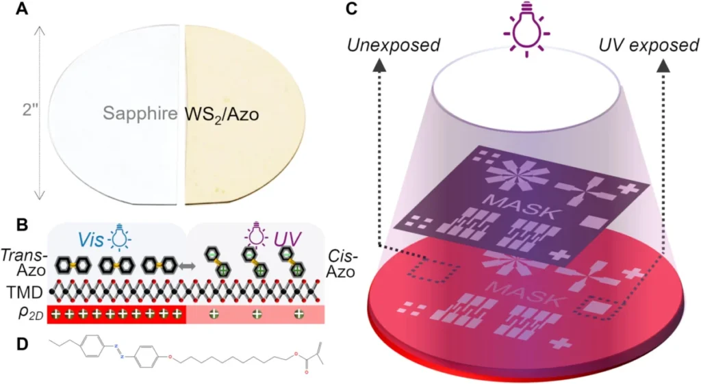
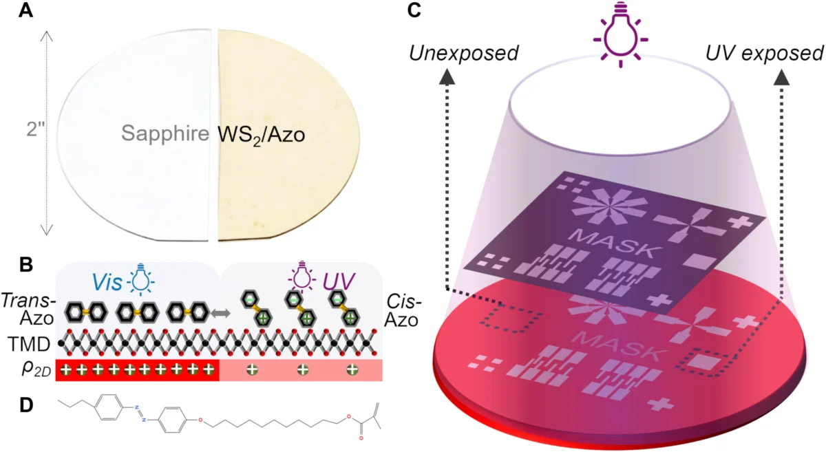
In the traditional landscape of microelectronics, the hardware we rely on—our processors, memory modules, and sensors—is physically "baked" into silicon. Once a transistor is fabricated, its threshold voltage, charge carrier mobility, and logic behavior are essentially immutable. However, a groundbreaking study published in Science Advances by a research team led by Jaehoon Ji has introduced a paradigm shift: the concept of an erasable, optically programmable semiconductor. By integrating azobenzene (Azo) compounds with transition metal dichalcogenide (TMD) monolayers, researchers have demonstrated that it is possible to dynamically alter the fundamental electrical properties of a transistor simply by toggling between different wavelengths of light.
Main Facts: The Physics of Light-Driven Transistors
At the core of this innovation lies the marriage of two distinct material classes: atomically thin semiconductors and photo-responsive organic molecules. The device architecture utilizes a TMD monolayer—specifically molybdenum disulfide (MoS₂)—which acts as the structural semiconductor. This material is then functionalized with azobenzene, a photochromic compound known for its ability to undergo a structural transformation when exposed to specific light frequencies.
When subjected to ultraviolet (UV) light, the Azo molecules undergo a trans-to-cis isomerization. This structural change alters the molecular dipole moment and the surrounding electrostatic environment of the underlying semiconductor. Because the TMD layer is only a few atoms thick, its electronic properties are highly sensitive to these external electrostatic influences. By switching the Azo molecules between their two states using UV and visible light, the researchers can effectively "reprogram" the charge carrier density of the field-effect transistor (FET), causing it to switch between n-type (electron-conducting) and p-type (hole-conducting) behavior or adjust its current-carrying capacity on the fly.
This is not merely a change in optical state; it is a fundamental alteration of the semiconductor’s electronic character. The device acts as a transistor whose logic gate characteristics are defined by the current light exposure rather than the doping levels established during manufacturing.
Chronology: A Path to Optically Programmable Logic
The realization of this technology is the culmination of years of iterative research into two-dimensional (2D) materials and photochromic molecular switches.
- Early Explorations (2015–2019): Research initially focused on the basic interaction between 2D material flakes and organic molecules. Early experiments established that simple surface functionalization could modulate the electrical resistance of MoS₂ flakes, but these interactions were often unstable or lacked the precision required for logical operations.
- The Integration Phase (2020–2023): Researchers began investigating the potential of using Azo compounds as "molecular gates." During this period, the stability of the photo-isomerization process was refined. The key challenge was ensuring that the molecular change didn’t degrade the underlying semiconductor lattice.
- The Breakthrough (2024–2026): The recent study by Jaehoon Ji and his team at Princeton University marks the first time these interactions were successfully leveraged to create a functional, reliable FET. By meticulously engineering the interface between the Azo-compound layer and the TMD monolayer, the team demonstrated repeatable switching cycles that maintained structural integrity over multiple exposures.
- Validation (September 2026): The publication of the findings in Science Advances provided the rigorous characterization necessary to prove that the device’s FET behavior was indeed a result of the Azo-mediated electrostatic gating, rather than simple thermal or parasitic effects.
Supporting Data: The Mechanics of Molecular Gating
The efficiency of this device is quantified by its ability to modulate the carrier density in the MoS₂ channel. In the study, the researchers observed a significant shift in the FET transfer characteristics upon UV irradiation.
Key Technical Metrics:
- Carrier Modulation: The device demonstrated the ability to shift the threshold voltage by several volts, a range sufficient to turn a logic-high state into a logic-low state without physical hardware modification.
- Spectral Selectivity: By alternating between UV light (which triggers the trans-to-cis switch) and visible light (which triggers the cis-to-trans reverse reaction), the system achieves a reversible "write-erase" cycle.
- Hysteresis Management: A critical hurdle in 2D electronics is the hysteresis observed in FET performance. The study highlights that the Azo-layer acts as a stable charge-trapping or charge-inducing buffer, which, under controlled optical input, actually helps stabilize the device’s behavior in its programmed state.
The research also notes that the device remains in its "programmed" state even after the light source is removed, effectively functioning as a non-volatile optical memory cell. This "write-once, read-many" capability is a significant departure from standard dynamic random-access memory (DRAM), which requires constant power to maintain data integrity.
Official Responses and Scientific Reception
The scientific community has reacted to the Princeton team’s findings with a blend of enthusiasm and cautious pragmatism. Experts in the field of optoelectronics have highlighted that while the proof of concept is robust, the transition from lab-scale devices to industrial-scale manufacturing faces significant hurdles.
In an official commentary accompanying the release, researchers noted: "The ability to tune the electrical properties of a transistor via light opens up a new dimension for circuit design. We are no longer limited by the doping profile established at the time of fabrication. However, the next step must address the longevity of the Azo-compounds when subjected to repeated switching over millions of cycles, as well as the scalability of deposition techniques for these monolayers."
Jaehoon Ji’s team has emphasized that their current focus is on "environmental stability." Because the Azo-compounds are organic in nature, they are susceptible to oxidation and moisture. Future iterations of the device will likely involve encapsulation techniques that allow light transmission while shielding the organic molecules from atmospheric degradation.
Implications: The Future of Dynamic Computing
The implications of this research are profound, potentially signaling the end of the "static hardware" era. By moving toward programmable semiconductors, the electronics industry could see a transformation in how we approach several key technological domains:
1. Programmable Logic Circuits
In traditional computing, an FPGA (Field Programmable Gate Array) uses physical switches (SRAM or Flash) to reconfigure its logic. These switches occupy significant silicon real estate. An optically programmable transistor could perform the same reconfiguration at the atomic level, leading to significantly higher logic density and reduced power consumption.
2. Neuromorphic Computing
Brain-inspired computing requires hardware that can adapt its synaptic weights. The ability to fine-tune the carrier density of a transistor using light provides a natural mechanism for simulating the plasticity of biological neurons. These devices could serve as the "memristors" of the next generation, enabling machines that learn and evolve their hardware configuration in real-time.
3. Smart Sensors
Imagine a sensor that can change its sensitivity or detection range depending on the environment. An optically programmable device could be tuned to detect specific chemical signatures or light frequencies, essentially allowing a single sensor package to function as an entire array of specialized detectors simply by updating its "programming" via an optical signal.
4. Hardware Security
Because these devices can be "erased" or reconfigured by specific light wavelengths, they offer a novel approach to hardware-level security. A device could be designed to self-destruct or reset its logic behavior if it detects unauthorized physical access or tampering, providing a layer of security that exists beneath the software stack.
Conclusion
The research presented by Ji et al. represents a fascinating convergence of organic chemistry and condensed matter physics. By demonstrating that the fundamental properties of a semiconductor can be steered by light, we are looking at the potential for a new category of "adaptive" electronics.
While we are currently in the experimental stage—with challenges ranging from long-term material stability to integration with existing CMOS fabrication processes—the door has been opened. As we move toward a future that demands increasingly flexible, efficient, and intelligent hardware, the ability to "write" logic onto a semiconductor with a pulse of light may prove to be one of the most significant advancements in post-silicon electronics. The next decade will determine whether these Azo-TMD structures remain a laboratory curiosity or evolve into the foundation for the next revolution in computing architecture.